Scoop has an Ethical Paywall


NCD Announces New Nano-Patterning Technologies
MEDIA RELEASE
8 August 2005
Nano Cluster Devices Announces New Nano-Patterning Technologies
Two new technologies for fabricating tiny electronic devices have been unveiled by Christchurch, New Zealand, based Nano Cluster Devices Ltd (www.nanoclusterdevices.com).
The first technology is a new variation on the techniques used by the semiconductor industry to produce computer chips. René Reichel, a PhD student who played a key role in developing the techniques, said, “Our new technique eliminates one of the processing steps that is currently needed to do lithography.”
The new technology can be used to produce patterns in almost any shape, and has been demonstrated by fabricating a tiny map of New Zealand, as well as electronic devices more than 1000 times smaller than the thickness of a human hair. All of NCD’s technologies are based on the assembly of clusters, which are particles with dimensions of a few billionths of a metre.
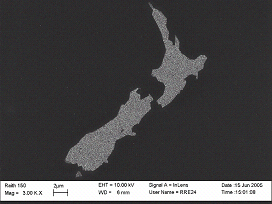
Map of New Zealand produced using NCD’s no-liftoff lithographyTM technique. About 100,000 of these maps would fit on the head of a pin. © Nano Cluster Devices Ltd 2005. Further images are available at http://www.nanoclusterdevices.com/index.cfm/Technology/no_liftoff.
The second technology is an improvement on stencilling techniques that are widely used in industry, but often suffer from problems where the stencils “clog”.
“It’s a bit like spray painting through a stencil, except that we are spraying clusters and not paint”, says Dr Jim Partridge who was the lead researcher on both projects. “By controlling the conditions so that the clusters do not stick to the stencil, we have shown that we can eliminate clogging and make very narrow wires.”
“These are really significant developments,” says NCD Chief Scientist Dr Simon Brown. “These new technologies allow faster and easier patterning of nanodevices, and may provide significant economic and technical advantages over existing technologies used by the semiconductor industry.”
The new technologies were developed by Jim Partridge, René Reichel and David Mackenzie in the Department of Physics and Astronomy at the University of Canterbury on behalf of NCD. NCD has filed patent applications on the new technologies in addition to those for its previously announced methods of self-assembling clusters (or nanoparticles) into nanowires.
Nanotechnology is an emerging field widely seen as having as great an importance as biotechnology and information technology. Nanotechnology will have tremendous impacts in these fields as well as in electronics, medicine and many others. NCD’s self-assembled nanowires could also be used as the key components in transistors or as interconnects between devices on silicon chips. Nanowires therefore have the potential to enable much smaller and faster computers than those possible today.
NCD’s Dr Brown has recently been invited to present at the prestigious NanoCommerce / SEMI NanoForum in Chicago in early November. Last month, NCD’s nanowire technology was showcased to the international semiconductor industry, after selection by a panel of industry experts for the Technology Innovation Showcase (TIS) in conjunction with the SEMICON West conference in San Francisco in July.
ENDS
About
Nano Cluster Devices Ltd.
Nano Cluster Devices Ltd was
formed in early 2003 to commercialize a unique combination
of top down and bottom up approaches to nano-technology. The
key aspect of the technology is that nano-wires can be
self-assembled between electrical contacts without the time
consuming and expensive manipulation that typically hinders
the production of nano-devices. For additional information
about Nano Cluster Devices Ltd., visit their website at
www.nanoclusterdevices.com.
Nano Cluster Devices Limited has developed novel methods for taking clusters of atoms and forming them into electrically conducting wires. These wires are so small they can only be seen with the aid of an electron microscope. They have a wide range of applications in many of the world’s multi-billion dollar industries. A comprehensive Patent Portfolio has been established.
 Stats NZ: Economic Impacts On New Zealand From Conflict In The Middle East – Report
 Advertising Standards Authority: ASA Annual Report 2025 - Platform-Neutral Regulation Keeps Pace With Digital Advertising
 Science Media Centre: Lead Pipes Banned For New Plumbing – Expert Reaction
 New Zealand Young Physicists Trust: Auckland To Host The ‘World Cup Of Physics’ In 2027; Search Begins For Student-Designed Tournament Logo
 Oxfam Aotearoa: Top CEO Pay Increased 20 Times Faster Than Workers’ Pay In 2025
 Bill Bennett: TUANZ Report - Networks Built, Value Missing